CCD-in-CMOS-based TDI imagers now UV-sensitive
The specialty imager broadens imec’s CCD-in-CMOS-based TDI imager portfolio, offered through various business models ranging from full-custom design to evaluation cameras.
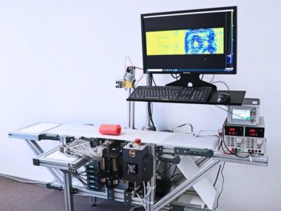
Imec’s TDI CCD-in-CMOS technology combines CCD TDI pixels and CMOS readout in one technology. This combination allows the best of both worlds to be realized on a single line-scanning imager: low-noise, highly sensitive TDI performance, and low-power, on-chip integration of fast and complex readout circuitry.
UV sensitivity is obtained by applying Imec’s backside illumination technology in combination with a dedicated antireflection coating. With backside illumination, light directly enters the imager from the backside, significantly enhancing the quantum efficiency of the image sensor. By adding a UV-specific antireflection coating, a high peak quantum efficiency of more than 70% is reached in the near-UV region of 250 to 400nm. Being sensitive to wavelengths smaller than the visible allows the imager to detect very small features – making the technology in particular attractive for semiconductor inspection applications, such as mask, wafer and particle inspection.
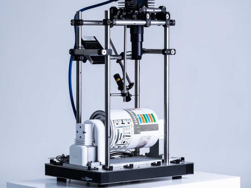
The TDI sensors are manufactured on 200mm wafers by using imec’s CCD process module inside its 130nm CMOS process flow. This cost-effective manufacturing flow is compatible with other wafer-level post-processing techniques such as spectral filter integration for enhanced TDI performance. The resulting image sensors have a high sensitivity and speed (up to 300kHz line rate) and have a low power consumption.
Imec – www.imec.be
 If you enjoyed this article, you will like the following ones: don't miss them by subscribing to :